Syntacore RISC-V MCU IP Features and Characteristics
1. Introduction
Choosing a RISC‑V processor core is a critical step that requires a thorough evaluation of multiple factors, including functional capabilities, performance, power consumption, physical dimensions and software compatibility. A systematic and balanced approach, based on the specific application requirements, ensures optimal configuration that meets both technical and business objectives.
Syntacore offers a state‑of‑the‑art RISC‑V processor IP portfolio, from 32‑bit compact MCU cores for deeply embedded applications to high-performance 64‑bit multicore clusters with memory coherency, SMP and Linux support. This article provides a detailed overview of Syntacore's updated RISC‑V microcontroller cores — SCR1, SCR3, SCR4 and SCR6.
The article will help engineers and SoC designers:
- Understand the technical characteristics of SCR microcontroller cores.
- Evaluate tradeoffs between performance, power consumption, area and functionality.
- Make well‑considered decisions when designing new devices.
2. Features and Applications
Syntacore's microcontroller-class IP portfolio features 4 configurable, silicon-proven, area-optimized processor cores: SCR1 (32‑bit), SCR3 (32/64‑bit), SCR4 (32/64‑bit) and SCR6 (64‑bit). These cores are tailored for diverse MCU applications, ranging from compact, energy-efficient embedded microcontrollers to high-performance systems for audio and image processing.
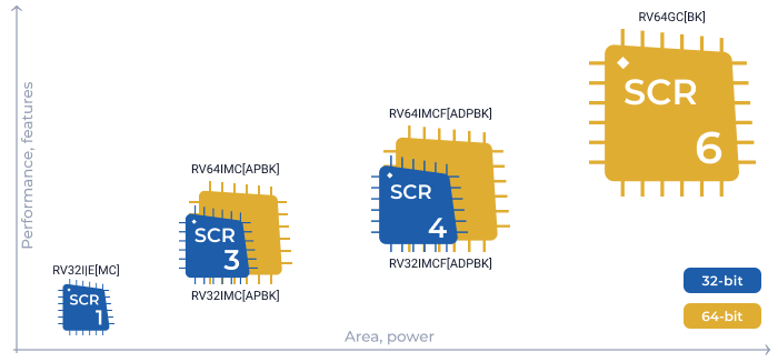
Figure 1. Syntacore's MCU IP portfolio.
- SCR1 — compact, entry-level 32‑bit microcontroller core with a 4‑stage in‑order pipeline. The core is optimized for a minimum area of less than 15k logic elements and open sourced under the SHL license, which permits commercial use.
- SCR3 — efficient 32/64‑bit microcontroller core with multicore support, DSP capabilities, a 5‑stage in‑order pipeline, a memory protection unit (MPU), and L1 and L2 caches.
- SCR4 — efficient 32/64‑bit microcontroller core with multicore support, DSP capabilities, a 5‑stage in‑order pipeline, a floating-point unit (FPU), a memory protection unit (MPU), and L1 and L2 caches.
- SCR6 — high-performance 64‑bit microcontroller core with multicore support, a 12‑stage out‑of‑order superscalar pipeline, a high-performance floating-point unit (FPU), a physical memory protection (PMP) unit, and L1 and L2 caches.
3. Architectural and Microarchitectural Criteria for Selecting SCR Cores
When selecting a microcontroller core, it is crucial to consider its functional characteristics, such as bit width, instruction set architecture (ISA), memory subsystem, interrupt controllers, and interfaces. The optimal choice involves a balance between sufficient functionality and minimizing system resource consumption.
3.1 Core features
Bit width
The SCR microcontroller IP portfolio comprises both 32‑bit (SCR1, SCR3, SCR4) and 64‑bit (SCR3, SCR4, SCR6) implementations, all fully compliant with RISC‑V specifications, enabling developers to choose the most suitable core tailored to the specific application needs.
Instruction Set Architecture (ISA)
The basic RISC‑V instruction set (RV32I(E)/RV64I), mandatory for all cores, provides essential integer operations (arithmetical, logical, memory access, CSR management, branching etc.), sufficient for simple control tasks. However, when designing SoCs for complex applications, support for specialized ISA extensions (e.g., bit manipulation or encryption) is critical, enabling more efficient execution of target computational workloads. SCR MCU cores support extensions that are fully compliant with the official RISC‑V architecture specifications:
- SCR1 — RV32I|E[MC]* Includes multiply/divide operations and compact instructions, ensuring minimal implementation complexity.
- SCR3 — RV[32|64]IMC[APBK] Includes multiply/divide operations, compact instructions and the A, P, B, K extensions (atomic, packed SIMD, bitwise operations and cryptographic functions).
- SCR4 — RV[32|64]IMCF[ADPBK] Includes multiply/divide operations, compact instructions, the F and D extensions for single- and double-precision floating-point calculations and the A, P, B, K extensions (atomic, packed SIMD, bitwise operations, and cryptographic functions).
- SCR6 — RV64GC[BK] Includes multiply/divide operations, compact instructions, atomic functions, F and D extensions for working with single- and double-precision floating-point calculations, as well as B, K extensions — bitwise operations and cryptographic functions.
*Optional extensions are indicated within brackets.
Letter encoding of extensions — I: Base Integer, E: Reduced Base Integer, M: Integer Multiplication and Division, A: Atomic Instructions, F: Single-Precision Floating-Point, D: Double-Precision Floating-Point, C: Compressed Instructions, P: Packed SIMD, B: Bit Manipulation, K: Scalar Cryptography, G — generic extension, that includes I, M, A, F, and D extensions.
For the latest, ratified RISC‑V ISA specifications visit: https://riscv.org/technical/specifications

Figure 2. RISC‑V architecture extensions.
Pipeline
A pipeline is a critical element of a processor core's architecture, determining its computational performance. SCR1, SCR3 and SCR4 cores feature an in‑order pipeline, enforcing sequential processing of instructions in program order. SCR1 features a 2–4 stage pipeline, offering a simple and compact design. SCR3 and SCR4 incorporate a deeper pipeline with 3–5 stages, enabling increased parallelism in execution.
SCR6 implements out‑of‑order execution, which dynamically reorders instructions to optimize computational unit utilization, and additionally supports a superscalar architecture enabling the simultaneous execution of multiple instructions per cycle. The core utilizes a deep pipeline (10–12 stages), providing increased throughput.
SMP
SCR cores operate effectively as standalone solutions for embedded systems, but can be combined into clusters to increase computing power and perform more complex tasks. SCR3, SCR4 and SCR6 microprocessor cores support coherent multi‑core configurations utilizing shared L2 cache, enabling seamless integration of different core types (e.g., 2xSCR3 + 2xSCR6). Clusters can include up to 8 cores, offering flexibility and scalability.

Figure 3. Example of a heterogeneous cluster based on SCR cores (MCU + APU).
Table 1. Key architectural and microarchitectural characteristics of SCR cores.
| Core Features | SCR1 | SCR3 | SCR4 | SCR6 |
|---|---|---|---|---|
| ISA | RV32I|E[MC] | RV[32|64]IMC[APBK] | RV[32|64]IMCF[ADPBK] | RV64GC[BK] |
| Pipeline, type | In‑order | Out‑of‑order, superscalar | ||
| Pipeline, stages | 2‑4 stages | 3‑5 stages | 10‑12 stages | |
| SMP support | – | Optional, up to 4 cores with coherency | Optional, up to 8 cores with coherency | |
3.2 Memory Subsystem
Caches and TCM
SCR MCU cores are equipped with an expandable memory subsystem that includes configurable sizes of TCM, L1 and L2 caches with coherency and error protection.
SCR1 supports a basic configuration with up to 64KB of TCM memory, ensuring fast access times critical for real‑time applications.
SCR3, SCR4 and SCR6 cores offer enhanced memory subsystem capabilities:
- SCR3/4/6 — TCM up to 256 KB with parity/ECC protection;
- Caches:
- SCR3/4 — L1: up to 32+32 KB (instructions/data) with parity/ECC protection; L2: 128–512 KB with ECC;
- SCR6 — L1: up to 64+64 KB with parity/ECC protection; L2: 128 KB–2 MB with ECC;
- Hardware cache coherency
- Integration into L3‑based clusters with CHI interface
Privilege Levels
The RISC‑V specification defines a hierarchical, multi‑level memory access scheme based on privileged and unprivileged modes, ranging from the lowest machine mode (M), responsible for core system functions and OS kernel management, to the hypervisor level (H), enabling task virtualization and secure execution in application-class processors running Linux.
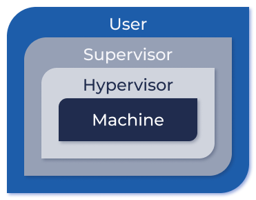
Figure 4. Privilege levels in the RISC‑V architecture.
SCR MCU cores offer robust isolation and privilege mode separation, with the SCR1 core providing separation at the machine (M) level, and SCR3, SCR4, and SCR6 cores additionally supporting user (U) mode, enabling versatile deployment in both bare‑metal and real‑time operating systems (RTOS) for sensitive applications. Hardware memory protection is enforced through the MPU, supporting up to 32 regions, in the SCR3 and SCR4 cores, and through the PMP module, capable of managing up to 64 regions, in the SCR6 core.
Table 2. SCR MCU Memory Subsystem Specifications.
| Features | SCR1 | SCR3 | SCR4 | SCR6 |
|---|---|---|---|---|
| Execution levels | M‑mode | U, M- modes | ||
| TCM | Up to 64KB | Optional, up to 256KB parity/ECC | ||
| L1 Cache | – | Optional, up to 64KB(I+D), parity/ECC | Up to 128KB(I+D), parity/ECC, stride data prefetcher support | |
| L2 Cache | – | Optional, 128KB to 512KB, ECC | 128KB to 2MB, ECC | |
| Memory Protection | – | MPU, up to 32 regions | PMP, up to 64 regions | |
3.3 Interfaces, Debugging and Interrupts
Interfaces and Debugging
SoCs demand high levels of component integration, fast data transfer capabilities and scalability to meet performance requirements. Additionally, the availability of debug interfaces is essential, enabling timely error detection and recovery, significantly improving the reliability, stability and quality of the entire system.
The SCR1 core utilizes standard AXI/AHB‑Lite buses with 32‑bit data transfer and features JTAG or cJTAG* debug interfaces. SCR3 and SCR4 support AHB/AXI data buses (up to 128‑bit wide), JTAG/cJTAG debug interfaces, a TCM AXI slave port for direct memory access and an L2 AXI coherent port for external accelerators integration. SCR6 supports AXI data width of up to 256 bits, ensuring high performance and support for complex systems with cached memory, a JTAG or cJTAG*-compatible debug interface, a TCM AXI slave port and an L2 AXI/ACE coherent port ensuring system scalability.
*Available upon request
Interrupt system
Interrupt controllers in SCR cores provide extensive capabilities for handling various types of interrupts, enabling efficient handling of tasks of varying complexity and specialization. SCR cores support the following types of interrupt controllers:
Core-level interrupt controllers:
- IPIC (Interrupt Programmable Interface Controller) — a local interrupt controller (up to 32 interrupt lines and 32 priority levels (based on interrupt ID)). Provides minimal latency, supports vectored interrupts and M and S modes.
- CLIC (Core-Local Interrupt Controller) — local interrupt controller (16 internal interrupts and up to 4080 external interrupt lines) supports programmable priorities (up to 256), vectored interrupts, and M and S modes. Provides the flexibility to configure different modes for each interrupt.
Platform-level interrupt controllers:
- PLIC/ACLINT
- PLIC — a cluster-level interrupt controller that aggregates and routes interrupts from peripheral devices to cores. Provides scalability and support for up to 1023 interrupt lines and up to 256 priority levels.
- ACLINT — inter-processor interrupt controller that generates system timer interrupts (MTIME/MTIMECMP), software interrupts (Machine Software Interrupt (MSWI) and Supervisor Software Interrupt (SSWI), supports up to 4096 interrupt lines.
- AIA (Advanced Interrupt Architecture) — APLIC + IMSIC*
- APLIC (Advanced Platform-Level Interrupt Controller) is a cluster-level controller with advanced interrupt routing and management capabilities and support for MSI (Message-Signaled Interrupts). It supports up to 1023 interrupt lines and up to 2047 unique interrupt identifiers per hart, dynamic routing, and programmable priorities, enabling flexible interrupt distribution in complex systems.
- IMSIC (Incoming Message-Signaled Interrupt Controller) is an interrupt controller integrated into APLIC. It maps interrupts to memory via dedicated registers, eliminating the need for traditional hardwired IRQ lines. It uses MSI messages for signaling, with interrupts delivered as writes to compact 4‑KiB memory pages and are immediately fed to the M/S level.
The SCR1 core supports a basic interrupt system based on the IPIC controller, capable of handling up to 16 interrupt lines and supporting up to 16 priority levels.
SCR3 and SCR4 cores offer advanced interrupt support: a modern CLIC controller managing up to 4096 interrupt lines and 256 priority levels, a PLIC capable of handling 1023 interrupts with 256 priorities, and an ACLINT controller supporting up to 4096 interrupt lines, including timer interrupts (in Machine mode) and software interrupts in Machine/Supervisor mode.
The SCR6 core features an advanced interrupt architecture, combining a PLIC similar to SCR3/4, supporting up to 1023 lines and 256 priority levels, alongside the innovative AIA system comprising the APLIC and IMSIC controllers. This integration enables handling of up to 1023 interrupt lines with support for 2047 unique identifiers, which significantly expands the system's capabilities in high-performance scenarios.
*Available upon request
Table 3. Overview of interfaces and interrupt controllers in SCR cores.
| Function/Core | SCR1 | SCR3 and SCR4 | SCR6 | |
|---|---|---|---|---|
| Interrupt Controllers | IPIC | Up to 16 interrupt lines, up to 16 priority levels (based on interrupt ID) | – | – |
| CLIC | – | Up to 4096 IRQs, up to 256 priority levels | – | |
| PLIC/ACLINT | – | Up to 1023/4096 IRQs, up to 256 priority levels | ||
| AIA (APLIC + IMSIC)* | – | – | Up to 1023 interrupt lines, up to 2047 distinct interrupt identities at each hart | |
| Bus Interface | AXI with 32‑bit data | AXI with 32/128‑bit data or an optional slave port | Cacheable AXI with 64/128/256‑bit data | |
| AHB‑Lite with 32‑bit data | AHB with 32/128‑bit data | Optional non-cacheable AXI with 64/128/256‑bit data | ||
| Debug Interface | JTAG or cJTAG* | |||
| Optional External Ports | – | TCM AXI slave port | ||
| Optional Coherent Interface | – | AXI L2 cache coherency port | AXI/ACE L2 cache coherency port | |
*Available upon request
Below is a summary table of SCR MCU cores, showcasing their key specifications and distinctive features.
Table 4. Summary of key characteristics of SCR MCU cores.
| Features | SCR1 | SCR3 | SCR4 | SCR6 |
|---|---|---|---|---|
| ISA | RV32I|E[MC] | RV[32|64]IMC[APBK] | RV[32|64]IMCF[ADPBK] | RV64GC[BK] |
| Pipeline, type | In‑order | Out‑of‑order, superscalar | ||
| Pipeline, stages | 2‑4 stages | 3‑5 stages | 10‑12 stages | |
| Execution Levels | M‑mode | U, M- modes | ||
| SMP Support | – | Optional, up to 4 cores with coherency | Optional, up to 8 cores with coherency | |
| FPU | – | – | SP and DP | High performance, SP and DP |
| TCM | Up to 64KB | Optional, up to 256KB parity/ECC | ||
| L1 Cache | – | Optional, up to 64KB(I+D), parity/ECC | Up to 128KB(I+D), parity/ECC, stride data prefetcher support | |
| L2 Cache | – | Optional, 128KB to 512KB, ECC | 128KB to 2MB, ECC | |
| Memory Protection | – | MPU, up to 32 regions | PMP, up to 64 regions | |
| Interrupt Controllers | IPIC – up to 16 interrupt lines, up to 16 priority levels (based on interrupt ID) | CLIC – up to 4096 IRQs, up to 256 priority levels | – | |
| PLIC/ACLINT – up to 1023/4096 IRQs, up to 256 priority levels | ||||
| – | AIA (APLIC + IMSIC)* up to 1023 interrupt lines, up to 2047 distinct interrupt identities at each hart | |||
| Interface Options | AXI, AHB‑Lite | AXI, AHB | AXI, ACE | |
| Debug Interface | JTAG or cJTAG* | |||
| Markets | IoT, smart home, control systems | Industrial, IoT, smart home | Industrial, IoT, mobile | Industrial, sensor fusion, image and audio processing |
*Available upon request
4. PPA Criteria for Selecting MCU SCR Cores
We previously discussed the functional capabilities of SCR cores, an essential but preliminary step in the selection process that ensures the core’s functionality aligns with the requirements of the SoC being developed. Given the high costs associated with tape‑out and the critical impact of errors, it is vital to understand the core’s physical parameters–power consumption (P), performance (P), and area (A)–early in the design process. PPA (Power, Performance, Area) analysis is employed to evaluate and optimize these parameters.
4.1 Performance
Frequency, performance and power are interdependent factors that collectively define the final product’s characteristics. In practice, a compromise must be found between these parameters, as maximizing one parameter can significantly degrade the other, thereby disrupting the balance. Table 5 shows the performance values obtained from synthetic benchmarks and core clock frequencies. These measurements are not final and are provided for reference purposes.
Table 5. MCU SCR performance and frequency.
| Parameter/Core | SCR1 | SCR3 (RV32/RV64) | SCR4 (RV32/RV64) | SCR6 |
|---|---|---|---|---|
| Dhrystone, per/MHz Obest (LTO) | 3,15 | 4,40/5,70 | 4,35/5,70 | 10,40 |
| Coremark, per/MHz Obest | 3,05 | 3,72/3,68 | 3,66/3,69 | 6,35 |
| Frequency, MHz (28 HPC+) | 1200+ | 1200+ | 1200+ | 1400+ |
Note 1: compilation conditions
- Coremark: LLVM‑20 ‑mcpu=scrX ‑O3 ‑funroll‑loops ‑finline‑functions ‑mllvm ‑‑enable‑dfa‑jump‑thread ‑falign‑functions=8 ‑falign-loops=4 ‑mllvm ‑scr‑loop‑streaming ‑mllvm ‑‑crc‑matcher=true ‑mllvm -enable-loop-int-wrap-predication=true
- Dhrystone: LLVM‑20 ‑ ‑mcpu=scrX ‑O3 ‑falign‑functions=8 ‑falign‑loops=4 ‑mllvm ‑riscv-enable-gep-opt=true ‑flto
Note 2: frequency measurement conditions
- Dhrystone 2.1_02, BM from TCM/L1
- LVT, Typical, 25C, 28HPC+
Note 3: SCR1 configuration – RV32IM, 3‑stage pipeline, TCM 32KB
4.2 Area and Power Consumption
In addition to performance, area and power consumption are equally important parameters. Area‑related data is a complex matter and depends on many factors, including memory capacity, IP core configuration and measurement conditions. For ease of understanding, we provide data only for the core logic for the most common 28 HPC process. These are approximate values, and for each specific task, our technical specialists are ready to help in meeting any (reasonable) target based on the technical capabilities of the cores.
Table 6. MCU SCR area and power consumption.
| Parameter | Description | SCR1 | SCR3 (RV32/RV64) | SCR4 (RV32/RV64) | SCR6 |
|---|---|---|---|---|---|
| Area, kGates | Core logic, from | 10 | 50/75 | 95/115 | 400 |
| Area, mm2 | Core logic, from | 0,004 | 0,016 | 0,026 | 0,10 |
| Power, uW/MHz | Dynamic (core logic), from | 1,40 | 2,73 | 3,00 | 13,20 |
Note 4: area and power measurement conditions
- Area: LVT @100MHz for 28HPC, no DFT
- Power: measured at post‑phys synthesis gate‑level netlist Dhrystone 2.1_02, 10 last iterations of 500, HVT, TYP @100MHz for 28HPC
The SCR1, with its excellent combination of performance, compact size and low power consumption, is ideal for simple embedded applications, including IoT, industrial and consumer devices.
SCR3 and SCR4 provide higher performance figures, an expanded feature set–with up to 5 pipeline stages, support for DSP operations, floating point capabilities (SCR4 only) and a compact size, making them suitable for more complex computing tasks, including smart home, IoT and industrial applications.
SCR6 offers the highest performance in Syntacore’s MCU portfolio. This is achieved through a superscalar architecture, a 12-stage dual-issue pipeline, support for a high-performance FPU, and a rich memory subsystem, making it ideal for highly loaded tasks, including industrial automation, image and voice processing, automotive, sensor fusion, smart home and smart city applications. It's also worth noting that its deeper pipeline enables higher clock rates, while the performance penalty associated with a longer pipeline is offset by the advanced architecture and microarchitectural solutions used.
5. Complete Development Platform with Regular Updates and Support
Previously, we discussed the hardware components of SCR cores and their microarchitectural features. However, hardware cannot function in isolation–comprehensive software support being also required. What's important is not just a set of software tools, but a complete suite permitting engineers to initiate projects swiftly and effortlessly, minimizing labor cost and accelerating the implementation process.
Syntacore provides a comprehensive software platform for SCR cores, featuring a preconfigured IDE based on modern toolchains, debugging tools, functional simulators and bootloaders, all integrated into a unified package. This solution provides end‑to‑end support for the entire development cycle–from initial prototyping to final device debugging–significantly accelerating time to market, through optimized integration of all components and guaranteed compatibility with the SCR processor core family. All components of the software package are regularly updated, ensuring access to the latest versions. Syntacore also provides ongoing support and professional consultations across the entire software spectrum, ensuring effective resolution of any issues that arise.
Syntacore software includes:
- Professional Software Development Suite (pre‑built GCC and microarchitecture optimized clang/LLVM toolchains, pre‑configured Eclipse and Visual Studio Code IDEs, QEMU simulation environment, BSP, debug tools and libraries)
- Essential System Software (a wide range of RISC‑V‑compatible tools and system software tested on SCR cores: pre‑configured Linux*, Zephyr, FreeRTOS operating systems, bootloaders, runtimes, and more)
- Fully‑featured FPGA SDK (based on the FPGA development boards from the leading vendors with a wide range of supported JTAG/cJTAG adapters)
*applicable only to APU‑class SCR cores – SCR5, SCR7, and SCR9
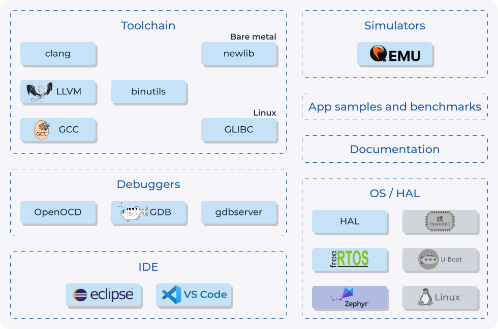
Figure 5. SC‑DT package contents (Zephyr OS is downloaded separately).
OpenSBI, U‑Boot, and Linux are applicable only to APU‑class SCR cores
6. Summary
Selecting a processor core is a complex, multi‑step process requiring a meticulous analysis of the application task being solved and careful selection of computational functions based on these requirements.
This article presented an in‑depth analysis of SCR microcontroller cores, covering essential features such as bit width, instruction set, pipeline architecture, memory subsystem, interrupt controllers and supported interfaces. It also explores key criteria for core selection, including benchmark results, area and power consumption, allowing for a more informed determination of optimal solutions for various applications.
Syntacore's updated SCR MCU core portfolio provides a comprehensive selection of IP, from compact, power‑efficient solutions to high-performance processors fully compliant with the RISC‑V architecture. Each core is designed to meet application requirements, delivering an optimal balance of performance, efficiency, and scalability:
- SCR1 is optimal for compact embedded systems in IoT, smart homes, and control systems where minimal area and power consumption are critical.
- SCR3 delivers balanced performance for IoT and industrial controllers, supporting both bare metal and RTOS operating systems.
- SCR4, with floating-point support, is designed for high-performance tasks in industrial IoT, and mobile applications.
- SCR6, with its superscalar pipeline, is designed for tasks requiring high computational power, such as image and audio processing, network processors and sensor fusion in complex embedded applications.