SCR1 RISC-V IP Overview: Key Features, Configurations, Performance Evaluation and Development Tools
1. Introduction
RISC-V enables open IP designs and provides access to modern processor technologies for both academic and commercial use. An example is the 32-bit, open-source, silicon-proven SCR1 core, developed by Syntacore. Introduced in 2017, the core has since been used in a number of projects – in commercial automotive, IoT and smart sensor applications, as well as in academic research and development.
The purpose of this article is to provide a comprehensive overview of the SCR1 core, review its architectural and microarchitectural characteristics and help developers and researchers make informed decisions about its use in their projects. The article also describes the core's available configurations, customization options, development tools, compares SCR1 with similar ARM IP cores and offers a detailed PPA evaluation.
2. Overview
SCR1 is a compact, 32-bit, energy-efficient microcontroller-class core. It has an area starting from just 10Kgates and is suitable for a wide range of domains, starting from general-purpose deeply embedded applications to industrial control and monitoring systems. Thanks to its open nature, the core can also be used for educational and academic purposes.
The core is based on a Harvard architecture with separate instruction and data buses, supports the RV32I/EMC instruction set, includes a configurable 2-4 stage in-order pipeline, an IPIC unit supporting up to 16 interrupts, TCM up to 64KB and industry-standard AXI4/AHB-Lite and JTAG/cJTAG* interfaces. SCR1 is fully compatible with the ratified specifications defined by RISC-V International.
*Available upon request
The SCR1 core is developed in SystemVerilog and distributed under the open source SHL license, allowing unrestricted commercial use. The core comes with pre-configured, tested and regularly updated software, detailed documentation, examples, projects and images for the popular FPGAs, allowing to get started right out of the box. Syntacore offers dedicated professional technical support on a commercial basis, ensuring rapid and seamless integration for your projects.
Technical Specifications
The following are the detailed technical specifications of the SCR1 core.
Table 1. Key technical parameters of the SCR1 core.
| Core | |
|---|---|
| ISA | RV32I/E[MC]*, Integer Multiplication and Division [M], Compressed Instructions [C] — optional |
| Execution Privilege Levels | Machine mode |
| Pipeline | In-order, 2 – 4 stage (integer) |
| Hardware Multiplier/Divider | Speed-optimized/area-optimized according to requirements (iterative or pipelined configuration depending on frequency and performance requirements) |
| Memory Subsystem | |
| Tightly-Coupled Memory (TCM) | I/D-shared, configurable: size — up to 64KB |
| Interrupt Subsystem | |
| Interrupt types | Direct/vector interrupts support |
| IPIC | Low interrupt latency, up to 16 interrupt lines, fixed interrupt priority levels support (based on interrupt ID), Machine-mode timer interrupt support, Machine-mode software interrupt support |
| Low Power Management | |
| Clock-gating support, power-gating support (coarse-grain power domain control, core-level UPF provided for low-power aware simulation and implementation), WFI (Wait for Interrupt) scheme to enter a sleep mode | |
| Debug Subsystem | |
| Interface | JTAG/cJTAG-compliant interface |
| Breakpoints | Up to 4 hardware breakpoints, unlimited software breakpoints support |
| Interfaces | |
| AXI | AXI4 AMBA standard interface |
| AHB | AHB-Lite AMBA standard interface |
| Timers and Counters | |
| Performance Monitoring | 2 performance counters |
| Embedded 64-bit RTC Timer | Machine-mode timer interrupt support |
*Optional extensions are given in parentheses. The letter coding for the extensions is I: Base Integer, E: Reduced Base Integer, M: Integer Multiplication and Division, C: Compressed Instructions.
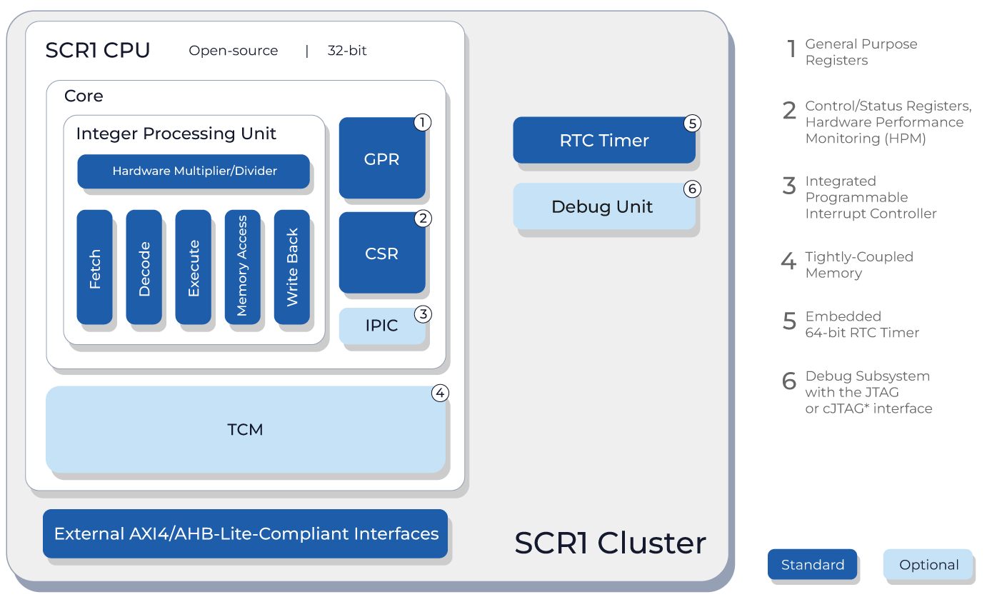
Figure 1. Block diagram of the SCR1 cluster.
Available Configurations
The SCR1 is available in three standard configurations — Min, Base and Max — providing a flexible set of features that can be adapted to meet the unique requirements of your specific application.
- The minimum (Min) configuration supports the RV32EC ISA, includes a two-stage pipeline and a TCM. This configuration features 16 general-purpose registers, making it suitable for deeply-embedded applications such as, for example, IoT sensors where minimal footprint is critical.
- The base (Base) configuration supports the RV32IC ISA, includes 32 general-purpose registers, a 3-stage pipeline, a TCM, an IPIC interrupt controller, support for vectored interrupt mode via the MTVEC register, a debug subsystem with a JTAG/cJTAG interface and 2 hardware breakpoints, offering an optimal balance of area efficiency and performance. This makes it suitable for general embedded applications like industrial control systems.
- The maximum (Max) configuration supports the RV32IMC instruction set, includes 32 general-purpose registers, a 4-stage pipeline, a hardware multiply and divide unit, extended debug functions with the JTAG/cJTAG interface (up to 4 hardware breakpoints), an IPIC interrupt controller and vectored interrupt mode via the MTVEC register, making ideal for high-performance embedded systems such as control systems and automotive electronics that demand maximum processing power.
Table 2. Key features and specifications of the SCR1 core configurations.
| Feature/Configuration | Min | Base | Max |
|---|---|---|---|
| Core | |||
| Area, kGates | 10 | 28 | 36 |
| ISA | RV32EC | RV32IC | RV32IMC |
| Pipeline Stages | 2 | 3 | 4 |
| Hardware Multiplier/Divider | — | — | + |
| Number of GPRs | 16 | 32 | 32 |
| Memory Subsystem | |||
| Tightly-Coupled Memory (TCM), up to 64KB | + | + | + |
| Interrupt Subsystem | |||
| IPIC | — | + | + |
| Interrupt lines | 1 | 16 | 16 |
| Vector interrupt support | — | + | + |
| Debug Subsystem | |||
| JTAG/cJTAG-compliant interface | — | + | + |
| Hardware Triggers | — | 2 | 4 |
Performance
The table below includes the basic PPA (performance, power and area) metrics for three SCR1 core configurations — minimum, base and maximum — using the widely adopted 90LP and 28HPC process technologies.
Table 3. SCR1 core performance characteristics.
| Parameter/SCR1 Config | Min | Base | Max |
|---|---|---|---|
| Dhrystone, per/MHz Obest (LTO)* | 2,85 | 3,14 | 2,86 |
| Coremark, per/MHz Obest** | 1,17 | 1,11 | 2,64 |
| Frequency, MHz (90LP) | 170+ | 270+ | 310+ |
| Frequency, MHz (28HPC) | 750+ | 1100+ | 1200+ |
Dhrystone 2.1, Coremark 1.0 run from TCM; SC-DT 2025.09, LLVM-20-sc *Obest with LTO; **Obest with ground rules
90LP, 9 track, LVT, typical, 1.2V, 25°C;
28HPC+, 12 track, LVT, typical 0.9V, 25°C;
Performance Comparison: SCR1 vs. ARM
The Table 4 below evaluates the performance and operating frequencies of SCR1 in comparison with ARM Cortex-M0 and M3 cores across 28HPC and 90LP process technologies.
Table 4. Key performance characteristics of SCR1 and ARM Cortex-M0, Cortex-M3 сores.
| Parameter/Core | SCR1 Max config | Cortex-M0 | Cortex-M3 |
|---|---|---|---|
| Dhrystone, per/MHz, Obest (LTO) | 2,86 | 1,91 | 3,49 |
| Coremark, per/MHz, Obest | 2,64/3,05 | 2,33 | 3,45 |
| Frequency, MHz (90 nm)* | 310+ | 268 | — |
| Frequency, MHz (28 nm)** | 1200+ | — | 891 |
*SCR1 — 90LP, 9 track, LVT, typical, 1.2V, 25°C; Cortex-M0 — 90LP, Arm SC7 RVT SS 1.08V, 125°C;
**SCR1 — 28HPC+, 12 track, LVT, typical 0.9V, 25°C; Cortex-M3 — 28HPM, 12 track, LVT, typical 0.9V, 85°C
SCR1 surpasses the ARM Cortex-M0 in performance, approaching Cortex-M3 levels. It can be further optimized by enabling the
SCR1_NO_DEC_STAGE define for Max configuration, which reduces the processor pipeline by one stage, allowing it to reach
Coremark scores of about 3,05 per MHz. Additionally, it offers some improvements in area efficiency and power consumption.
Area and Power Efficiency
The Table 5 below provides characteristics for the 90LP process technology.
Table 5. Area and power efficiency of SCR1 and ARM Cortex-M0, Cortex-M3 cores.
| Parameter | SCR1* | ARM** | |||
|---|---|---|---|---|---|
| Min, from | Base, from | Max, from | Cortex-M0, min | Cortex-M3, min | |
| Area, mm2 | 0,0027 | 0,07 | 0,091 | 0,03 | 0,09 |
| Power, uW/MHz | 5,82 | 10,18 | 9,96 | 12,5 | 31 |
*Area — 90LP, 9 track, LVT, typical 1.2V, 25°C @50MHz, core logic only;
Power — 90LP, 9 track, LVT, worst 1.08V, 125°C @50MHz;
**Cortex-M0 — min configuration, 90LP, 7 track, typical 1.2V, 25°C, 125°C;
***Cortex-M3 — min configuration, 90LP, 7 track, RVT, typical 1.2V, 25°С
3. Configuration Options
On top of standard configurations there is number of architectural and microarchitectural features that can be fine-tuned to better meet the requirements of a specific application. In addition, Syntacore provides comprehensive services and support, including architectural and microarchitectural tuning, ISA configuration and compiler optimizations ensuring optimal implementation adapted to specific project requirements.
The following are key configuration options available for adapting SCR1 to diverse application needs (overall design includes more than 40 configurable options).
Table 6. SCR1 configuration options.
| Feature | Description |
|---|---|
| Core | |
| ISA | RV32(I/IM/IMC/E/EM/EMC) |
| Pipeline Stages | 2/3/4 (based on frequency requirements) |
| Hardware Multiplier/Divider | Speed-optimized/area-optimized according to requirements (iterative or pipelined configuration depending on frequency and performance requirements) |
| Number of GPRs | 16/32 |
| Memory Subsystem | |
| Tightly-Coupled Memory (TCM) | 4KB to 64KB |
| Interrupt Support | |
| IPIC | Up to 16 interrupt lines, fixed interrupt priority levels support based on ID (up to 16), direct/vectored interrupt mode |
| Low Power Management | |
| Clock-gating support, power-gating support (coarse-grain power domain control, core-level UPF provided for low-power aware simulation and implementation), WFI (Wait for Interrupt) scheme to enter a sleep mode | |
| Debug Subsystem | |
| Debug unit | Debug subsystem with the JTAG/cJTAG interface, hardware triggers support |
| Number of Hardware Triggers | Up to 4 |
| Interfaces | |
| 32-bit AXI4 or AHB-Lite external interface | |
| Timers and Counters | |
| Performance Monitoring | 2 performance counters (cycle counter, retired instructions counter) |
| Embedded 64-bit RTC Timer | Machine-mode timer interrupt support |
4. Complete Development Platform
In addition to the SCR1 core and HW collateral, Syntacore provides a full set of pre-configured and tested tools that significantly boost productivity and simplify the development workflow.
Professional Software Development Suite
Syntacore Development Toolkit (SC-DT) is a comprehensive solution for developers that includes GCC/LLVM-based toolchains, an integrated development environment with support for Visual Studio Code and Eclipse, GDB and openOCD debuggers, a QEMU simulation environment, a bootloader, system software, sample applications, benchmarks and detailed documentation.
In addition, Syntacore provides extensive support for third-party debugging hardware and software from leading vendors: SEGGER, Lauterbach, Ashling, Digilent, Olimex.
Table 7. SC-DT components and supported 3rd party tools.
| SC-DT | ||
|---|---|---|
| Feature | Description | |
| IDE | Visual Studio Code plugin | |
| Eclipse | ||
| Toolchain | GCC with binutils and Newlib libraries | |
| clang/LLVM compiler | ||
| Debuggers | GNU GDB | |
| OpenOCD | ||
| Simulator | QEMU | |
| Software Examples | Sample applications and benchmarks | |
| HAL and BSP | ||
| OS | FreeRTOS/(RTEMS/Zephyr)* | |
| Bootloader and Firmware | First-stage bootloader | |
| Documentation | User Guide, Tools Guide (IDE, CLI) | |
| Third-Party Tools | ||
| SEGGER | Probe | J-Link Ultra+ |
| IDE | Embedded Studio | |
| Lauterbach | Probes | PowerDebug |
| PowerTrace | ||
| Debugger | Trace32 | |
| Ashling | Probe | Opella-XD |
| IDE | RiscFree™ | |
| Digilent | Probe | JTAG-HS2 |
| Olimex | Probes | ARM-USB-TINY-H |
| ARM-USB-OCD-H | ||
*Downloaded separately
FPGA SDK
The FPGA SDK is a ready-to-use project that includes an IP core, peripheral modules, standard interfaces, memory and the ability to add custom peripherals for testing on a specific board.
The SDK includes pre-built images, a bootloader, an OS (Zephyr), tests, HAL and BSP, as well as the Eclipse or Visual Studio development environments.
Off-the-shelf projects are available for the most popular FPGA boards*:
- Digilent Arty (Xilinx)
- Digilent Nexys4DDR (Xilinx)
- Altera Arria-V (Intel)
- Terasic DE10-Lite (Intel)
*Boards from other manufacturers can be considered upon request.
All SDKs for these boards are available on the GitHub repository, ready to install and configure and are continually supported by Syntacore.
Documentation
The SCR1 package includes comprehensive documentation:
- User Manual with detailed technical specifications, configuration guidelines and operational instructions
- External Architecture Specification (EAS) Manual, providing an in-depth description of the SCR1 architecture and microarchitecture, including components, ISA and interfaces
- FPGA SDK Guide, offering step-by-step instructions for FPGA setup, image loading and application development tailored to specific boards
5. Summary
This article describes main architectural and microarchitectural features of the open-source SCR1 core, presents its PPA characteristics, compares it with similar ARM cores, describes development tools and provides an overview of the supported FPGA boards.
Fully compliant with the ratified RISC-V specifications and distributed under the open-source SHL license, SCR1 allows unrestricted use in both commercial and academic applications.
SCR1 is available in three default out-of-the-box configurations — Min, Base and Max — and offers flexible options for further fine-tuning. SCR1 can be customized with the help of our professional team to meet your specific requirements, making it suitable for a wide range of domains — from general-purpose embedded and Internet of Things (IoT) to control and monitoring systems.
SCR1 delivers competitive PPA results compared to similar ARM Cortex-M0 and Cortex-M3 IP cores. The core comes with fully pre-configured tools, an FPGA SDK and detailed documentation for a quick start with professional SLA-based support available.